


Earlier this year, Intel got a new CEO and kicked off a new business plan that would open its foundries to other chip-design firms, just like how TSMC and Samsung Semiconductor operate. At its “Intel Accelerated” event today, the company laid out a roadmap for its future as a for-hire foundry. Besides the future of ever-smaller process nodes, the company also announced it has scored one of the world’s biggest chip designers, Qualcomm, as a future foundry customer.
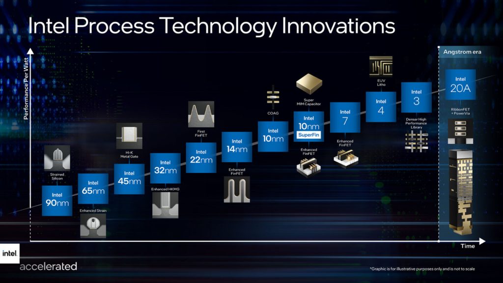
As part of entering the foundry market, Intel will start naming its process nodes more like its rivals. The process-node numbers used for chips like “5nm” started out life as a measurement of transistor size, but eventually the marketers got hold of them and companies started cheating down their numbers to look more advanced. Intel says its new naming scheme will better align with how TSMC and Samsung talk about their foundry technologies. Gone are the days of “Intel 10nm Enhanced Super Fin”—instead, the node is called “Intel 7.” It should have a comparable density to the TSMC and Samsung 7 nm nodes and will be ready for production in Q1 2022 (TSMC and Samsung are currently shipping “5nm” products). “Intel 4″—which Intel previously called “7nm”—is now said to be equivalent to TSMC and Samsung’s 4 nm node, and it will begin manufacturing products in 2023.
If you’re wondering what happens when we run out of “nm” numbers, Intel’s sales pitch for that is the “Angstrom” era, a unit of measurement that is one-tenth of a nanometer. In 2024, the company wants to ramp up the “Intel 20A” process node (so a “2nm” equivalent, but Intel was calling this node “5nm” previously, but remember these are marketing numbers and not really units of measurement). In early, 2025 the company will be working on “Intel 18A.”
The name change to “Intel 20A” instead of “2nm” seems to partly be because that process node will include some major architectural changes for Intel’s chips. For years, the company has used FinFET transistors, but for Intel 20A the company will switch to a gate-all-around (GAA) design it’s calling “RibbonFET.” FinFETs would scale channel current capacity by adding multiple fins and, therefore, more horizontal space. But GAA designs allow chip manufacturers to stack multiple channels on top of each other, making current capacity a vertical problem and increasing chip density. Intel 20A will also introduce “PowerVias,” a new chip-design method that will put power delivery on the backside of the chip. This design would put the power-delivery layer on the bottom of the chip, then the transistors, then the communication wires. Traditional chip design puts the transistors at the bottom, and higher-up signal and power layers have to intermingle to reach the transistor layer.
If Intel actually manages to stick to its roadmap, it should be able to count Qualcomm as an interested customer. President and CEO Cristiano Amon expressed interest in the “20A” node saying, “Qualcomm is excited about the breakthrough RibbonFET and PowerVia technologies coming in Intel 20A. We’re also pleased to have another leading-edge foundry partner enabled by IFS [Intel Foundry Services] that will help the U.S. fabless industry to bring its products to an onshore manufacturing site.”
Today, Qualcomm makes a lot of chips and is a customer of both TSMC and Samsung. The two companies regularly compete for each new design in Qualcomm’s lineup, with industry reports often describing a down-to-the-wire horse race of one beating the other. Whether or not Intel will be in the mix for most of these foundry battles depends on if it can catch up to TSMC and Samsung. At least now, Qualcomm is offering Intel a spot in the race, instead of smartphone irrelevance.


