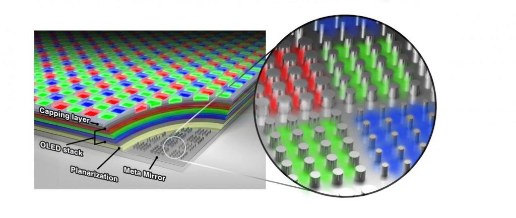
By expanding on existing designs for electrodes of ultra-thin solar panels, Stanford researchers and collaborators in Korea have developed a new architecture for OLED—organic light-emitting diode—displays that could enable televisions, smartphones and virtual or augmented reality devices with resolutions of up to 10,000 pixels per inch (PPI). (For comparison, the resolutions of new smartphones are around 400 to 500 PPI.)
Such high-pixel-density displays will be able to provide stunning images with true-to-life detail—something that will be even more important for headset displays designed to sit just centimeters from our faces.
The advance is based on research by Stanford University materials scientist Mark Brongersma in collaboration with the Samsung Advanced Institute of Technology (SAIT). Brongersma was initially put on this research path because he wanted to create an ultra-thin solar panel design.
“We’ve taken advantage of the fact that, on the nanoscale, light can flow around objects like water,” said Brongersma, who is a professor of materials science and engineering and senior author of the Oct. 22 Science paper detailing this research. “The field of nanoscale photonics keeps bringing new surprises and now we’re starting to impact real technologies. Our designs worked really well for solar cells and now we have a chance to impact next generation displays.”
In addition to having a record-setting pixel density the new “metaphotonic” OLED displays would also be brighter and have better color accuracy than existing versions, and they’d be much easier and cost-effective to produce as well.
Hidden gems
At the heart of an OLED are organic, light-emitting materials. These are sandwiched between highly-reflective and semi-transparent electrodes that enable current injection into the device. When electricity flows through an OLED, the emitters give off red, green or blue light. Each pixel in an OLED display is composed of smaller sub-pixels that produce these primary colors. When the resolution is sufficiently high, the pixels are perceived as one color by the human eye. OLEDs are an attractive technology because they are thin, light and flexible and produce brighter and more colorful images than other kinds of displays.
This research aims to offer an alternative to the two types of OLED displays that are currently commercially available. One type—called a red-green-blue OLED—has individual sub-pixels that each contain only one color of emitter. These OLEDs are fabricated by spraying each layer of materials through a fine metal mesh to control the composition of each pixel. They can only be produced on a small scale, however, like what would be used for a smartphone.
Larger devices like TVs employ white OLED displays. Each of these sub-pixels contains a stack of all three emitters and then relies on filters to determine the final sub-pixel color, which is simpler to fabricate. Since the filters reduce the overall output of light, white OLED displays are more power-hungry and prone to having images burn into the screen.
OLED displays were on the mind of Won-Jae Joo, a SAIT scientist, when he visited Stanford from 2016 to 2018. During that time, Joo listened to a presentation by Stanford graduate student Majid Esfandyarpour about an ultrathin solar cell technology he was developing in Brongersma’s lab and realized it had applications beyond renewable energy.
“Professor Brongersma’s research themes were all very academically profound and were like hidden gems for me as an engineer and researcher at Samsung Electronics,” said Joo, who is lead author of the Science paper.
Joo approached Esfandyarpour after the presentation with his idea, which led to a collaboration between researchers at Stanford, SAI and Hanyang University in Korea.
“It was quite exciting to see that a problem that we have already thought about in a different context can have such an important impact on OLED displays,” said Esfandyarpour.
A fundamental foundation
The crucial innovation behind both the solar panel and the new OLED is a base layer of reflective metal with nanoscale (smaller than microscopic) corrugations, called an optical metasurface. The metasurface can manipulate the reflective properties of light and thereby allow the different colors to resonate in the pixels. These resonances are key to facilitating effective light extraction from the OLEDs.
“This is akin to the way musical instruments use acoustic resonances to produce beautiful and easily audible tones,” said Brongersma, who conducted this research as part of the Geballe Laboratory for Advanced Materials at Stanford.
For example, red emitters have a longer wavelength of light than blue emitters, which, in conventional RGB-OLEDs, translates to sub-pixels of different heights. In order to create a flat screen overall, the materials deposited above the emitters have to be laid down in unequal thicknesses. By contrast, in the proposed OLEDs, the base layer corrugations allow each pixel to be the same height and this facilitates a simpler process for large-scale as well as micro-scale fabrication.
In lab tests, the researchers successfully produced miniature proof-of-concept pixels. Compared with color-filtered white-OLEDs (which are used in OLED televisions) these pixels had a higher color purity and a twofold increase in luminescence efficiency—a measure of how bright the screen is compared to how much energy it uses. They also allow for an ultrahigh pixel density of 10,000 pixels-per-inch.
The next steps for integrating this work into a full-size display is being pursued by Samsung, and Brongersma eagerly awaits the results, hoping to be among the first people to see the meta-OLED display in action.


