Kesterite (Cu2ZnSnS4, CZTS) is a sulfide mineral with a unique lattice structure that can be considered as derived from chalcopyrite CuInSe2 (CIS) by substituting two atoms of In3+ in the chalcopyrite by one atom of Zn2+ and one atom of Sn4+. The elements included in this mineral and its derivatives Cu2ZnSn(S,Se)4 (CZTSSe) are less-toxic and abundant on Earth, which could be very advantageous for the development of more sustainable and low-cost technologies.
Over the past few decades, material scientists and engineers have been exploring the possibility of using kesterite materials to create more affordable and sustainable solar cells. Despite extensive efforts in this direction, the highest power efficiency attained by kesterite solar cells is 12.6%, which was first reported in 2013.
Researchers at Nanjing University of Posts & Telecommunications, Fudan University, the Chinese Academy of Sciences and University of Washington have recently surpassed this decade-long record, developing a better performing kesterite/CdS interface that could enable the creation of solar cells with a 13% efficiency. This interface, presented in a paper published in Nature Energy, could enable the creation of more efficient and better performing kesterite solar cells.
“The Nature Energy paper builds on our previous work, which showed that the kesterites Cu2ZnSn(S,Se)4 (CZTSSe) and (Ag,Cu)2ZnSn(S,Se)4 (ACZTSSe) absorbers fabricated from SnCl4 based DMSO solution show improved device performance with the reduced recombination near kesterite/CdS interface,” Hao Xin, one of the researchers who carried out the study, told TechXplore. “The primary objective of the Nature paper was to understand the original of the defective heterojunction interface of kesterite/CdS and how thermal annealing greatly reduces the concentration of the defects.”
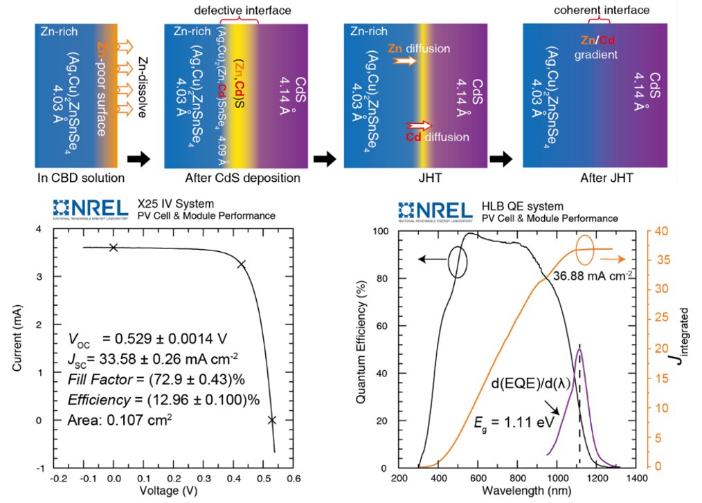
In their experiments, Xin and his colleagues showed that a kesterite/CdS heterojunction is constructed on a Zn-poor surface, as Zn2+ dissolves during the chemical bath deposition process. As a result, Cd2+ occupies site previously occupied by Zn and Zn2+ is re-deposited into CdS, resulting in a defective interface with a lattice mismatched.
To reconstruct the epitaxial interface, the researchers applied a technique known as low temperature annealing on the kesterite/CdS junction. This technique allowed them to drive the migration of Cd2+ from the absorber layer back to the CdS site and Zn2+ from the absorber bulk to the material’s surface.
“The precursor films (fabricated from SnCl4 based DMSO solution) have kesterite (Cu2ZnSnS4, CZTS) structures already formed, which takes a direct phase transformation grain growth mechanism to form CZTSSe/ACZTSSe absorber films during selenization,” Xin said. “Our approach avoids secondary phases and thus creates a uniform and less defective absorber.”
The researchers evaluated the kesterite/CdS interface they created in a series of tests and found that it outperformed previously created kesterite interfaces. Their initial fabrication method was found to significantly improve the open-circuit voltage and fill factor of solar cell devices, achieving certified efficiencies of 12.96% over a small-area (0.11cm2) and 11.7% over a large-area (1.1cm2).
In the future, the experimental methods devised by Xin and his colleagues could enable the development of kesterite/CdS interfaces with more uniform absorber films. These interfaces could in turn be used to develop better performing kesterite solar cells.
“For the first time, we unveil how the kesterite/CdS heterojunction is constructed (based on Zn-poor surface) and why it is defective (due to occupation of Cd2+ on Zn vacancy), which contrast with CIGS, from which kesterite is inherited,” Xin added. “In our next works, we plan to further engineer the defects of kesterites.”