Van der Waals (vdW) dielectrics, materials with dielectric properties and affected by van der Waals forces, are commonly integrated within electronic devices, as they can help to preserve the properties of 2D semiconducting materials. So far, however, fabricating these materials and integrating them with semiconductors has proved challenging, mainly because synthesizing them required sophisticated techniques, such as mechanical exfoliation or vapor deposition processes.
Researchers at Huazhong University of Science and Technology and other institutes in China have recently devised an alternative strategy to fabricate vdW dielectrics on the wafer scale, using an inorganic molecular crystal film. This strategy, introduced in a paper published in Nature Electronics, opens new possibilities for the fabrication of wdW films, which could in turn lead to the development of various highly performing 2D devices.
“This paper was initially inspired by one of our previous research works,” the researchers who carried out the study, told TechXplore via email. “In 2019, we published a paper in Nature Communications. In that work, we reported the growth of ultrathin Sb2O3 crystalline flakes.”
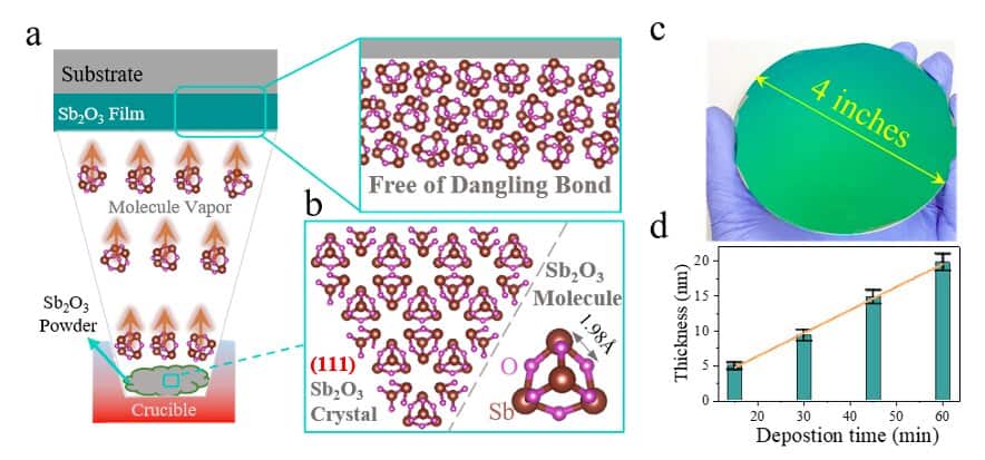
The ultrathin crystalline flakes introduced by Tianyou Zhai and his colleagues in their previous work have a unique and very interesting structure, which differs significantly from the layer structure of 2D materials, such as graphene and MoS2. Instead of being arranged in layers, Sb2O3 crystals are composed of tiny molecules with caged structures, which are all connected to each other through vdW interactions.
“When we realized the difficulties in integrating dielectric materials with 2D semiconductors to construct high-performance devices, we started thinking about the possibility of using our inorganic molecular crystals,” the researchers said. “The goal of our recent study was to address this longstanding issue in the development of 2D devices.”
Van der Waals dielectrics are essentially dielectric materials that do not have dangling bonds on their surface. Zhai and his colleagues found that this absence of dangling bonds ultimately allows their integration with 2D semiconductors and thus their use for the development of highly performing devices.
“We took advantages of the special crystal structure of inorganic molecular crystals,” the researchers explained. “The small molecules can be evaporated easily without the structural loss because of the weak vdW interaction. This means that molecules are sublimed during the evaporation deposition process and these evaporated molecules then deposit on the target substrate, forming a film.”
In contrast with most previously proposed strategies for fabricating dielectrics, the fabrication method devised by Zhai and his colleagues is scalable and can easily be used to produce wafer-scale films. In addition, it greatly simplifies the integration of vdW dielectrics with 2D materials.
“I think the most important achievement of this work is that we developed a totally new approach to address an important issue in our research field, the field that focuses of 2D materials,” the researchers said. “By using the special structure of inorganic molecular crystals, we developed a new approach to fabricate vdW films.”
In the future, the new fabrication approach could enable the large-scale production of highly performing devices based on 2D semiconductors. Notably, the thermal evaporation strategy they devised is also compatible with current complementary metal-oxide-semiconductor (CMOS) fabrication processes.
When developing the new fabrication method, Zhai and his colleagues drew inspiration from the unique molecular structure of the Sb2O3 crystalline flakes reported in their previous work. Therefore, so far, they only applied it to these flakes.
In their future works, they hope to identify other inorganic materials with similar structures and potentially more advantageous properties, such as larger bad gaps, dielectric constants, and breakdown voltages, as well as lower current leakage rates. This could help to increase the performance of 2D devices even further.
“Hopefully, in our next studies we can identify a similar material that can support the fabrication of 2D devices that exhibit comparable performance to the state-of-the-art Si MOSFET,” the researchers added. “Meanwhile, we are also trying to study the fundamental properties of this kind of vdW film, especially for that with thickness of nanometer scale. Since the publication of our work, some researchers contacted with us and asked us to collaborate with us. We can’t predict what we can do in the future when our efforts are combined with other researchers’ ideas, yet we feel that we will be conducting many studies in the near future.”
